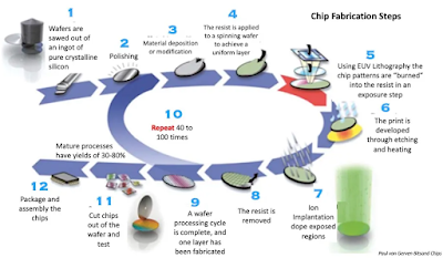
The transistors inside a digital chip are in nanometers scale. The electron travelling doped semi conducting part is in the order of several nanometers. The main purpose of the rest of the semiconductor on a wafer is to form a mechanical base and insulate electron flow. I propose this doped semi conducting part to be created individually for each transistor. Therefore, larger chips can be more economically build in real 3d, transistor above another transistor would be possible. Creating each transistor individually may look like a slow process but single machine chip manufacturing can be a reality and overall chip manufacturing speed would be higher. Microchips are made by building up layers of interconnected patterns on a semiconducting wafer. The microchip manufacturing process involves hundreds of steps and can take up to four months from design to mass production.


No comments :
Post a Comment